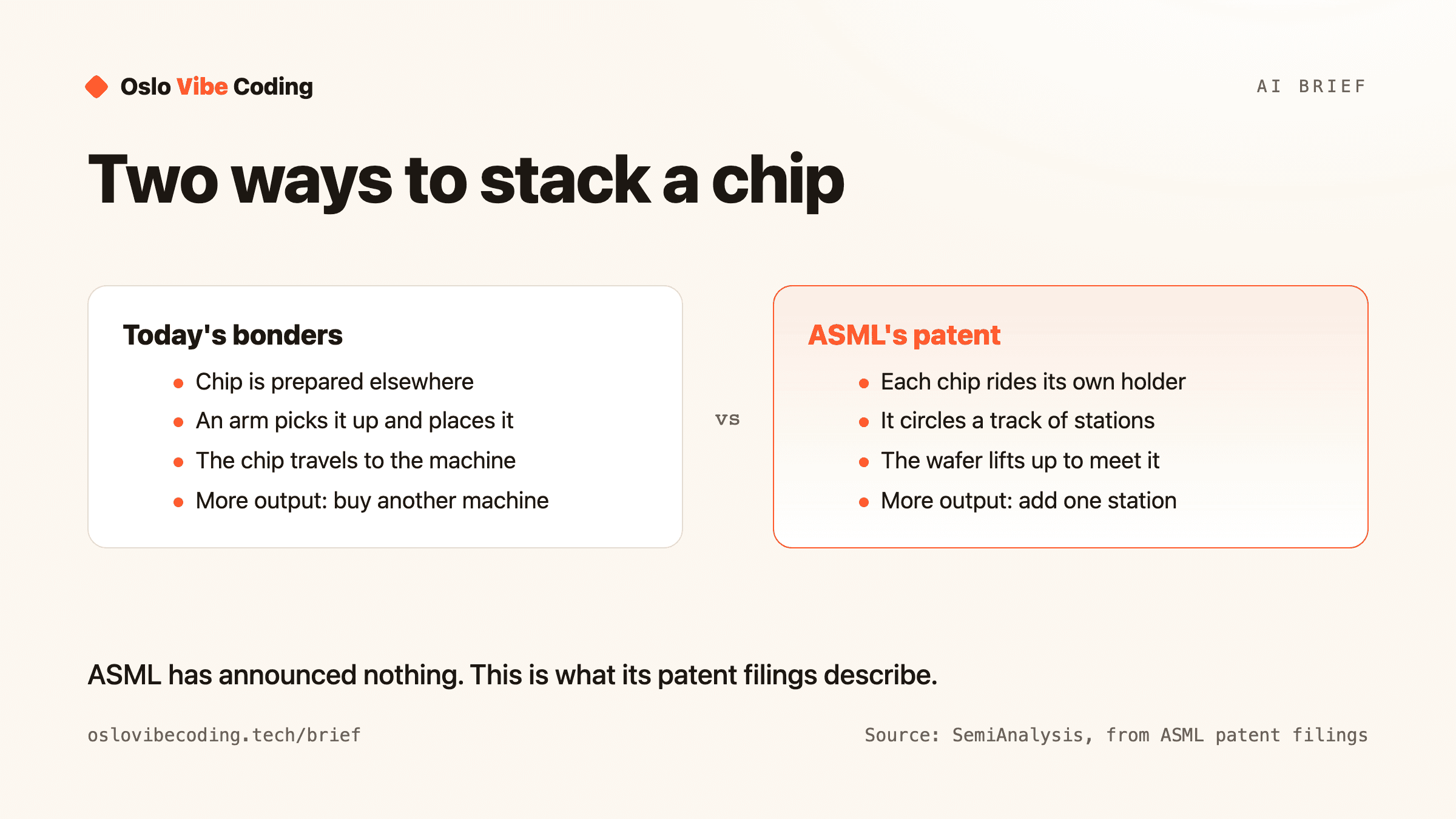
ASML, the Dutch company that is the only maker of the EUV lithography machines used to print the most advanced chips, appears to be building a hybrid bonding tool, a machine that joins chips face to face so they can be stacked. ASML has not announced such a product. The evidence, set out by the research firm SemiAnalysis in October 2026, is 27 bonding patent families filed between December 2022 and November 2024, a March 2026 report in the Korean trade paper The Elec that ASML had begun designing a hybrid bonder with its suppliers Prodrive Technologies and VDL ETG, and ASML's own 2024 investor-day roadmap, which lists hybrid bonding. The main patent (WO2025201788A1) describes an unusual design: each chip rides its own holder around a track past cleaning and measuring stations, and the wafer is lifted up to meet it. Today's market leader for this kind of tool is another Dutch company, Besi. SemiAnalysis expects makers of advanced processors such as TSMC and Intel to adopt an ASML tool first, and expects HBM, the stacked memory used with AI chips, not to switch to this method before 2029, if at all. Patents are not products, and the hardest engineering problems are still open.
What happened
ASML is a Dutch company most people have never heard of, and almost every phone, laptop and AI chip depends on it. It is the only company that makes EUV lithography machines (the bus-sized tools that print the tiniest patterns onto silicon). If you want to make a leading-edge chip, you buy from ASML.
In October the chip research firm SemiAnalysis published an analysis arguing that ASML is quietly preparing to enter a second business: hybrid bonding, the technique used to stack chips on top of each other. ASML itself has announced nothing. The case rests on its patent filings, one news report, and a slide from its own investor day.
The facts
First, the jargon. For decades chips got better by shrinking: smaller transistors (the tiny switches inside a chip), more of them per square millimetre. Shrinking is getting slower and more expensive, so the industry is also building upwards, placing one chip on top of another. Hybrid bonding is the cleanest way to do it. Two chips are pressed face to face so that thousands of tiny copper pads on one meet the matching pads on the other, with no solder in between. AMD has sold processors with memory stacked this way since 2022, under the name V-Cache.
The evidence. SemiAnalysis counts 27 bonding patent families (a family is one invention filed in several countries) from ASML between December 2022 and November 2024, most of them for die-to-wafer bonding, which means placing individual chips onto a full silicon wafer. Later filings are not public yet. In March the Korean trade paper The Elec reported that ASML had started designing a hybrid bonder with two of its long-time Dutch suppliers, Prodrive Technologies and VDL ETG. And ASML's 2024 investor-day roadmap already lists hybrid bonding for memory and processors.
The design. Today's machines work like a very precise robot arm: a chip is cleaned and prepared elsewhere, then a bond head picks it up and places it. ASML's main filing (WO2025201788A1) describes something different. Each chip sits on its own small holder and rides around a track. It stops at stations for inspection, cleaning, surface treatment and measurement, and at each stop the tool moves in to the chip. At the last station the wafer is lifted up to within a few hundredths of a millimetre, the holder nudges the chip into its final position, and the two are pressed together.
Why it is so hard. The chip must land within about 50 nanometres of its target, roughly a thousandth of the width of a human hair. And the surfaces must be almost perfectly clean. SemiAnalysis notes that a single speck one micrometre across (a hundredth of a hair) trapped between two wafers can stop them bonding across an area about 10 millimetres wide. It also says the current tools manage at most about one wafer an hour in today's uses, which keeps costs high.
The chip has to land within a thousandth of the width of a human hair.
The everyday version
Think of a workshop where one master craftsman builds a watch from start to finish, walking to fetch each part. Now think of an assembly line, where the watch moves past a row of specialists and each does one job. The line is not more skilled. It is better organised: every specialist is always busy, and if one step is slow you add a second person at that step instead of building a second workshop.
That is the idea in the patent. Because every chip travels on its own holder, a slow step such as cleaning can have three stations while a fast step has one, and nothing waits. SemiAnalysis points out a second benefit: switching to a different kind of chip becomes a software setting, which suits packages that mix several chip types.
The reason ASML might be good at this is that the two hardest problems, lining things up to the nanometre and keeping dust away, are the same two problems it has spent decades solving in its printing machines. SemiAnalysis is careful here: ASML's precision figures come from lithography, not from a working bonder.
Is this actually new?
ASML widening its reach is not new. According to SemiAnalysis it bought Cymer for light sources in 2013, HMI for inspection in 2016 and Berliner Glas for optics in 2020, and in 2025 it shipped its first machine for chip packaging (the step where finished chips are assembled into the part you actually buy).
Hybrid bonding is not new either. It is already used in volume for phone camera sensors and flash memory, and another Dutch company, Besi (BE Semiconductor Industries), is the only supplier with tools in volume production for the chip-by-chip version. What would be new is the company with the tightest grip on chip printing also selling the machine for chip stacking, and selling the two as a pair that share measurements.
Keep the usual caution about patents. Companies patent many things they never build. A filing shows what engineers were thinking about, not that a product exists, works, or will ship.
What it means
For the AI tools you use, nothing changes this year. This is plumbing, several steps removed from a chatbot. It matters because stacking is one of the main ways chips are expected to keep improving once shrinking slows, and faster, cheaper stacking would feed into the processors and memory that AI runs on.
Who is affected. SemiAnalysis expects makers of advanced processors, mainly TSMC and Intel, to be the first buyers, and calls the move bad news for Besi, whose bonding business is concentrated at those two customers. It also expects HBM (the fast memory stacked next to AI chips) not to adopt this chip-by-chip method before 2029, if at all. Those are one research firm's forecasts, not facts.
Measured caveats. ASML has confirmed nothing. The detailed part of the SemiAnalysis analysis, on the problems ASML still has to solve, sits behind its paywall; the free part names them: measuring each chip accurately enough before it lands, the moment of contact itself, adapting the cleaning and measuring tools to work on a moving track, and keeping the whole loop free of dust. For Europe it is worth noticing that the two companies at the centre of this story, ASML and Besi, are both Dutch. Watch for an announcement from ASML, or for a first tool arriving at a customer for testing. Until then, this is a well-argued reading of patent drawings.
A patent shows what engineers were thinking about, not that a product exists.
Curious about AI? Come build with us.
Oslo Vibe Coding runs free, beginner-friendly drop-ins where we build real things with AI. No one codes alone.