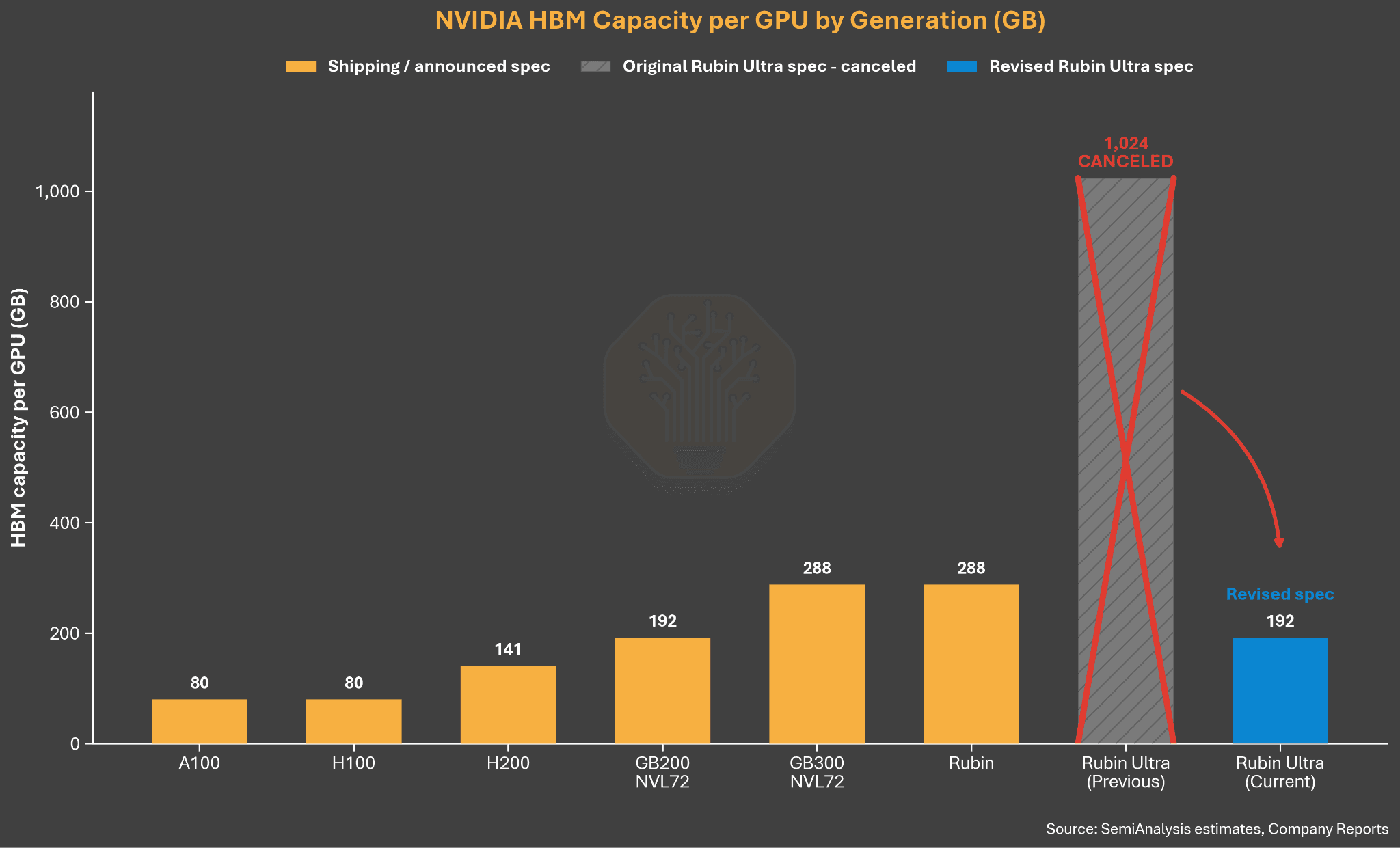
Every generation of Nvidia's AI chips has carried more HBM (high bandwidth memory, the stacks of memory chips bonded next to the processor) than the last: 80 gigabytes on the A100 and H100, 141 on the H200, 192 on the GB200, 288 on the GB300 and on Rubin. Rubin Ultra was previewed at 1,024 gigabytes. According to SemiAnalysis, which first reported the change, the version that ships will carry 192, and the whole industry is moving from memory stacks 12 chips tall to 8, a year after it expected to go to 16. The main reason is supply: there are not enough HBM wafers to make the number of 12-high stacks Nvidia's chip orders for next year would need, and memory is now the most expensive component in the box. The second reason is that it may not matter. A memory stack delivers the same bandwidth whether it is 4, 8 or 12 chips tall, because the 2,048 data wires are the same; what you pay for is the gigabytes. And most AI work today is answering users, which is limited by how fast memory can be read, not how much there is. A rack of 72 GB300 chips holds about 21 terabytes of HBM; the largest open model, Kimi K3 at 2.8 trillion parameters, needs less than 8% of that. Rubin Ultra's rack links 576 chips together, an eightfold increase that more than offsets a third less memory on each. SemiAnalysis argues 4-high stacks will be the best value for inference from the next memory generation on. This is their analysis; Nvidia has not published the revised figure.
What happened
For as long as Nvidia has made AI chips, each new one has carried more memory than the last. The chart above is the whole history. The A100 and H100 shipped with 80 gigabytes of HBM (high bandwidth memory, explained below). The H200 was the same processor with 141. The GB200 has 192, the GB300 has 288, and Rubin, the chip due next year, also has 288. When Nvidia previewed Rubin Ultra, the chip after that, it showed a terabyte: 1,024 gigabytes per package.
According to SemiAnalysis, the chip-industry research firm that first reported the change, the Rubin Ultra that actually ships will carry 192 gigabytes. That is less than Rubin, less than the GB300, and the first time in recent memory that Nvidia's next flagship holds less than the one it replaces. Part of the gap is that the previewed version was to have four compute dies (the processor chips themselves) and the shipping version has two. Even allowing for that, SemiAnalysis says memory per compute die drops from 256 gigabytes to 96.
Behind the headline number is a change in how the memory is built. HBM comes in stacks, and the industry has been climbing: 8 chips tall, then 12, with 16 expected next. SemiAnalysis says the next generation of accelerators is standardising on 8-high stacks instead of 12, and that the supply chain is now preparing for that. Its report, "Long Live the Short King", was published on 13 September; two of its authors, Myron Xie and Jordan Nanos, walked through it on the SemiAnalysis podcast the next day. Nvidia has not published the revised specification, so treat the 192 figure as SemiAnalysis's reporting, not an announcement.
SemiAnalysis: "For the first time in recent memory, NVIDIA's next flagship will have less capacity than the one it replaces."
What HBM is, and why height does not equal speed
An AI chip has two jobs: do the arithmetic, and fetch the numbers to do it on. The fetching is the hard part. Ordinary computer memory (DRAM, the same kind in your laptop) is cheap and roomy but the connection to it is too slow. So AI chips use HBM: several DRAM chips stacked on top of each other like floors in a building, bonded right next to the processor, connected by 2,048 tiny wires. The industry calls one stack a cube, and describes it by height: 4-high, 8-high, 12-high.
Here is the detail the whole story turns on. The 2,048 wires belong to the cube, not to each floor. They are shared out among the floors, with a maximum of 512 per floor. So a 4-high stack already uses all 2,048 wires, and adding floors adds gigabytes without adding a single wire. In the coming HBM4E generation, each floor holds 4 gigabytes, so a 4-high stack is 16 gigabytes, an 8-high is 32 and a 12-high is 48. All three deliver the same bandwidth (the rate at which data can be read), about 3,328 gigabytes per second per cube.
Now the money. Memory makers price a cube mostly by how many gigabytes it holds. But what an AI chip gets value from is mostly the bandwidth. So a shorter stack gives you the same speed for a lot less money, which is why SemiAnalysis calls choosing lower stacks "almost a free lunch". The only question is whether you can live with fewer gigabytes. Until recently the answer was no. The report's argument is that the answer has just changed.
The first reason: there are not enough wafers
SemiAnalysis is clear that the decision was "in large part motivated by supply". HBM is made on the same DRAM wafers as ordinary memory, and it eats far more wafer per gigabyte. As AI chips took an ever-larger share of those wafers, the report says, the result was "the extreme DRAM shortage we see ourselves in today". For next year, Nvidia has secured a certain amount of processor capacity at TSMC (the world's main chip factory) and of the advanced packaging that joins processor and memory together. It has not secured enough HBM to put 12-high stacks on all of it. "There are simply not enough wafers," the report says. Moving to 8-high yields far more cubes from the same limited wafers and closes the gap.
Cost pushes the same way. The report says HBM prices rise sharply next year, that memory is now Nvidia's largest component cost, and that even with demand far above supply Nvidia is having to give up some margin as those costs climb. Shorter stacks are cheaper stacks.
What this means for the memory makers, SK Hynix, Samsung and Micron, is subtler than it sounds. They sell fewer gigabytes per chip, but far more cubes, and SemiAnalysis frames the shift as a "win-win" for the labs' costs and the suppliers' profitability. That is the firm's argument rather than a reported fact, and the suppliers have not commented.
The second reason: most AI work is reading, not storing
The report divides AI computing into three buckets. Pre-training (building a model from scratch) needs lots of memory capacity, because the chip has to hold the model's weights plus all the working figures of the training run. Inference (the model answering users) is different: to produce each word, the chip must read every active parameter of the model plus the user's conversation so far, and it does that for every single word. That is limited by how fast memory can be read, not by how much there is. Reinforcement learning, the final training stage that now dominates progress, behaves like inference. And the share of the world's AI computing spent on pre-training has shrunk, so the majority of it is now bandwidth-limited.
Capacity still matters, up to a threshold: a system must hold the model and the users' conversations. Above that, extra gigabytes are dead weight you paid for. The report's illustration: at 100 words per second, a cube's 3,328 gigabytes per second of bandwidth gives you 33 gigabytes of reading per word. A 48-gigabyte 12-high cube cannot be fully read in that time; the last 15 gigabytes sit there, unused and expensive. SemiAnalysis calls this stranded capacity.
And the threshold has moved, because memory is now pooled across a whole rack. In the H100 era, one server held 8 chips and 640 gigabytes of HBM; the best open model of the day, Llama 3.1 at 405 billion parameters, took 63% of that just for its weights, which is why the H200's extra 61 gigabytes per chip mattered so much. A GB300 NVL72 rack links 72 chips into one system with about 21 terabytes of HBM. The largest open model today, Kimi K3 at 2.8 trillion parameters, needs 1,561 gigabytes in its compressed 4-bit form, under 8% of the rack. Rubin Ultra's rack, NVL576, links 576 chips, an eightfold jump that "more than offsets the one third reduction in HBM capacity per GPU". The report says hardware teams at the frontier labs now want 4-high stacks for their own chip programmes from the HBM4 generation on, because that is where tokens per memory wafer, like tokens per watt, is maximised.
The everyday version
Picture a water tank on your roof feeding a single pipe to the kitchen. The pipe is the bandwidth: it can deliver 33 litres a minute, no more. The tank is the capacity. The plumber's price list charges by the litre the tank holds, not by the pipe, because the pipe is the same on every tank.
For years your household kept growing, so you kept buying a bigger tank, and you needed every litre. Then two things changed. The town built a shared reservoir feeding all the houses on the street, so no single tank has to hold much. And it turned out most of what you do is make tea, which only cares how fast water comes out of the tap. Now the sensible thing is the smallest tank that still fills the pipe. Nvidia has, by this account, stopped buying the big tank.
Is this actually new?
A flagship with a smaller headline number than its predecessor is rare, but it is not unprecedented, and the precedent is encouraging. In the early 2000s Intel chased ever-higher clock speeds with the Pentium 4, until heat and power made the number meaningless; in 2006 it launched the Core chips with lower clock speeds that did more useful work per watt, and the headline number never came back. The lesson was that the spec sheet number people compared was not the one that determined value. SemiAnalysis's case is that gigabytes per chip is that number for HBM: it was the right thing to chase when a model barely fit on a server, and it stops being the right thing once a rack holds twelve copies of the model.
What is new is the direction of the memory industry's roadmap. Less than a year ago, SemiAnalysis notes, the expectation was 16-high stacks and beyond. Now the standard is going the other way. That is the kind of reversal that ripples through factory plans, and it is why the report reads as much as a message to memory suppliers as to chip buyers.
What to take from it
If you want one sentence: the fast memory on AI chips is scarce enough that Nvidia is cutting it, and the way AI is used today means that may cost almost nothing.
For anyone outside the chip industry, the useful idea is the split between capacity and bandwidth, because it comes up everywhere: in phone storage, in broadband, in the difference between a big hard drive and a fast one. AI has just discovered, at industrial scale, that it had been paying for capacity and using bandwidth.
Three things to watch. Whether Nvidia confirms the 192-gigabyte figure when it next talks about Rubin Ultra, since the whole story rests on SemiAnalysis's reporting so far. What SK Hynix, Samsung and Micron say about 8-high and 4-high in their next results, because a change in stack height is a change in their factory plans. And whether the DRAM shortage this report describes starts showing up in the price of the memory in ordinary laptops and phones, which is where most people would first feel it.
Curious about AI? Come build with us.
Oslo Vibe Coding runs free, beginner-friendly drop-ins where we build real things with AI. No one codes alone.